Micro LED Mass Transfer Market: By Product Type (Electrostatic Power Adsorption, Liquid Assembly Transfer, Elastomeric Print Film Transfer, and Laser); Application (Small Size Applications (Mobile Phones), Mid-size Applications (Tablets, Laptops), Large Size Applications (TV), and Ultra-large Commercial Screens); Region—Market Size, Industry Dynamics, Opportunity Analysis and Forecast for 2026–2035
- Last Updated: 11-Dec-2025 | | Report ID: AA0823568
Market Snapshot
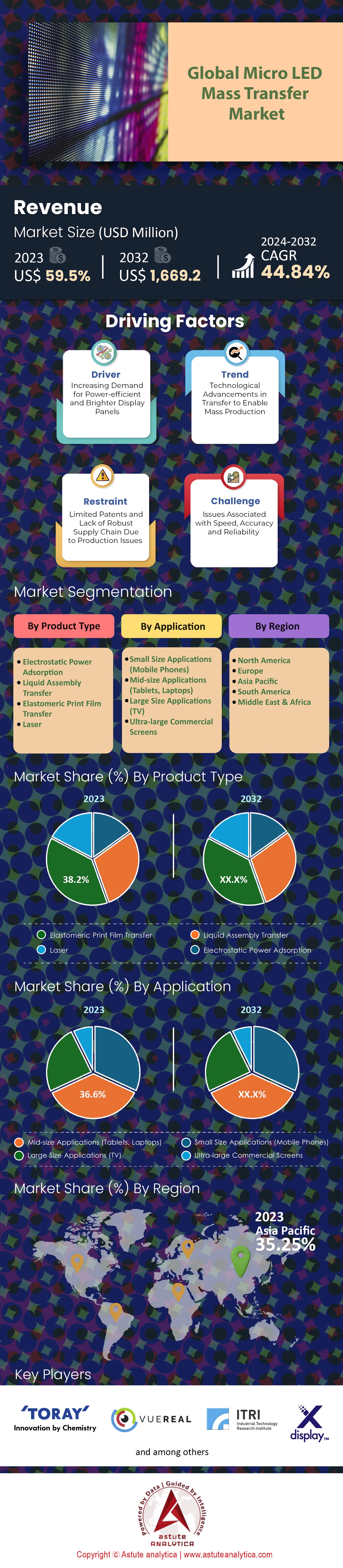
Micro LED mass transfer market was valued at US$ 110.7 million in 2025 and is projected to attain a market size of US$ 4,498.3 million by 2035 at a CAGR of 44.84% during the forecast period 2026–2035.
Key Findings in Micro LED Mass Transfer Market
- In terms of the product type, elastomeric print film transfer held over 38% revenue share of the market.
- Based on application, mid-size applications, such as tablets and laptops, hold the dominant position in the market with over 36.2% market share.
- Asia Pacific captures over 35.25% of revenue share of the market.
The micro LED mass transfer market has fundamentally shifted by late 2025, moving from a speculative research phase into early-stage commercialization. While the exit of Apple from its in-house watch project in early 2024 initially sent shockwaves through the industry, the market has successfully pivoted toward a more diversified ecosystem. Industry data from late 2025 indicates that nearly 30 wafer fabs and pilot lines are now active globally, with the aggregate market scale pushing toward the RMB 100 billion mark. The narrative has changed from "if" mass transfer works to "how efficiently" it can scale. Stakeholders are witnessing a pragmatic maturation where yield rates are finally stabilizing near the critical 99.99% threshold in pilot environments, driven by heavy capital expenditure from Chinese and Taiwanese consortiums.
Profitability is no longer a theoretical horizon for the leading players in the micro LED mass transfer market. For instance, companies like PlayNITRIDE have reported profitable quarters in 2025, signaling that the unit economics of the market are beginning to align with commercial reality. The focus has narrowed significantly on solving the "last mile" transfer costs, which previously accounted for over 40% of the display price. As production lines in Xiamen and Taoyuan ramp up, the industry is entering a "golden window" of opportunity where technological deployment and market demand are reinforcing each other.
To Get more Insights, Request A Free Sample
Why Are Laser Technologies Decimating Mechanical Alternatives In High Volume Lines?
The demand within the micro LED mass transfer market is overwhelmingly concentrated on laser-based transfer technologies, specifically Laser Lift-Off (LLO) and Laser Induced Forward Transfer (LIFT). Operational data confirms that these non-contact methods are the only viable solutions for achieving the requisite throughput of 100 million chips per hour needed for consumer electronics. Unlike stamp-based picking, which struggles with the adhesion physics of chips smaller than 10µm, laser systems offer the precision required for the new generation of bezel-less displays. Coherent’s UVtransfer platforms have become the industry benchmark, effectively marginalizing slower mechanical alternatives in high-volume settings.
Fluidic assembly and stamp transfer technologies retain a niche demand for specific low-density applications, but the momentum is clearly with laser solutions. Manufacturers are prioritizing tools that can handle "epilayer-only" dies to reduce material costs. The market is witnessing a surge in orders for "all-in-one" transfer tools that integrate inspection and repair capabilities directly into the laser line. This consolidation of process steps is a direct response to the "yield-repair trap," proving that speed alone is insufficient without guaranteed placement accuracy.
What are the Two Critical Applications Fueling The Current Demand Explosion?
The unprecedented appetite for high-brightness, transparent displays in the automotive sector is a primary engine fueling the micro LED mass transfer market. Automakers are aggressively adopting transparent Micro LED screens for side windows and "morphing" center control units, which require transparency levels exceeding 60% and brightness over 5000 nits to compete with direct sunlight. Traditional OLEDs cannot survive the thermal and brightness requirements of a vehicle cabin, leaving Micro LED as the sole contender for next-generation cockpits.
Wearable technology acts as the second pillar of this demand surge. Although Apple, one major player exited, the broader smartwatch market has accelerated, driven by the need for outdoor visibility and battery efficiency. New product launches in 2025, such as high-end adventure watches, utilize Micro LED to achieve pixel densities above 326 PPI while maintaining lower power consumption than OLED. Furthermore, the explosion of AI-integrated smart glasses has created a scramble for ultra-compact micro-displays, pushing the micro LED mass transfer market to innovate in sub-5µm transfer accuracy for Augmented Reality (AR) applications.
Which Four Nations are Currently Architecting Global Supply Chain?
China stands as the volume leader in the micro LED mass transfer market, utilizing its dominance in the LCD supply chain to pivot rapidly into Micro LED. The nation’s strategy involves aggressive capacity expansion to lower the cost per pixel, making them the primary source for mid-tier display panels. Taiwan follows closely as the innovation hub, where the "pure-play" transfer foundries are located. Taiwanese firms excel at the complex system integration required to marry Micro LEDs with TFT backplanes, serving as the bridge between chipmakers and global brands.
South Korea occupies the third spot, driven by vertically integrated giants that create the end-market demand. Their role is pivotal in setting the quality standards for TV and wearable panels, effectively acting as the "kingmakers" for transfer technology vendors. The United States ranks fourth, not as a panel producer, but as the dominant supplier of the critical laser and inspection equipment. US-based companies like Coherent and KLA provide the "arms" for this display revolution, supplying the high-precision tools that Asian fabs rely on to function.
Are Smart Cockpits and AR Glasses the True Killer Applications For Mass Adoption?
Recent adoption trends indicate that automotive "Smart Cockpits" are the fastest-growing application segment for the micro LED mass transfer market. Tier-1 automotive suppliers are moving beyond prototypes to mass production of panoramic Heads-Up Displays (HUDs) and transparent A-pillar screens. These applications demand robust transfer technologies capable of bonding LEDs to non-conventional, often flexible or curved, substrates. The ability to display critical driving data on a transparent surface without obstructing the driver's view is a killer application that only Micro LED can deliver reliably.
Augmented Reality (AR) glasses represent the second wave of rapid adoption. The 2025 launch of consumer-ready AI glasses by major tech firms has necessitated a shift toward "LEDoS" (Micro LED on Silicon) technologies. While this often involves wafer-level bonding rather than pick-and-place, the demand for hybrid transfer solutions to combine RGB arrays onto a single optical engine is soaring. The micro LED mass transfer market is expanding to include these ultra-fine pitch requirements, creating a new sub-sector dedicated exclusively to near-eye display manufacturing.
Who are The Equipment Giants Powering the Transition To Mass Production?
Coherent Corp remains the formidable leader in the equipment space, providing the UVtransfer laser systems that define modern high-speed manufacturing. Their ability to execute Laser Lift-Off and Forward Transfer in a single workflow has made them indispensable to major fabs. PlayNITRIDE has evolved from a startup to a market cornerstone, offering not just chips but a "Micro LED 3D Printer" service that allows clients to bypass the steep learning curve of transfer technology. Their profitability in 2025 validates their unique business model.
Toray Engineering continues to dominate the inspection and repair segment of the micro LED mass transfer market. Their equipment, which integrates photoluminescence testing with rapid laser repair, is the standard for maintaining yields above the six-nines requirement. Rounding out the top tier is ASMPT, which provides the critical bonding backend solutions. Their mastery of interconnect technologies ensures that once chips are transferred, they remain electrically connected, a vital step that often bottlenecks competitors.
What Strategic Milestones In 2025 Have Redefined The Competitive Landscape?
The landscape of the micro LED mass transfer market was redefined in June 2025 when Xiaomi launched its AI Smart Glasses, which sold out instantly. This event marked the first mass-consumer validation of Micro LED in the AR space, proving that the technology could meet aggressive price points. In the same quarter, Tianma Microelectronics announced the successful commissioning of its fully integrated Micro LED production line in Xiamen. This facility, utilizing full-laser mass transfer, represents one of the first lines capable of bezel-less tiling without size limitations.
Another significant development occurred when PlayNITRIDE finalized a USD 21 million deal to build a dedicated production line for AUO. This partnership cements the trend of "Fab-in-Fab" models, where transfer experts embed their technology directly into panel manufacturers' facilities. Additionally, Aledia unveiled its breakthrough 3D Nanowire technology at CES 2025, solving the "Red LED efficiency" problem that has plagued the industry for a decade. These milestones collectively signal that the technical hurdles of the micro LED mass transfer market are being systematically dismantled.
How Will AI and Hybrid Packaging Reshape The Future of Mass Transfer?
The most prominent trend closing out 2025 is the aggressive integration of Artificial Intelligence into the mass transfer workflow. Manufacturers are deploying AI-driven "Smart Transfer" algorithms that dynamically adjust laser fluence and placement coordinates in real-time based on the topology of the donor wafer. This reduces the reliance on costly redundancy schemes, allowing manufacturers to move from a 2:1 pixel redundancy to a 1.1:1 ratio, saving millions in material costs. The micro LED mass transfer market is becoming as much about software intelligence as it is about hardware precision.
Opportunities are also expanding in the "Micro LED in Package" (MIP) sector. By packaging LEDs before transfer, manufacturers can utilize larger, easier-to-handle units, effectively lowering the barrier to entry for TV manufacturers. This shift allows traditional LED display makers to enter the Micro LED space without purchasing ultra-precision laser tools, widening the total addressable market. Stakeholders who invest in these hybrid packaging-transfer technologies stand to capture significant value as the industry bifurcates into "ultra-precision" (AR/Watch) and "modular mass" (TV/Auto) segments.
Segmental Analysis
Elastomeric Print Film Transfer Leading Through Precision and Speed
When it comes to product type, elastomeric print film transfer held over 38% revenue share. The micro LED mass transfer market currently relies on elastomeric techniques due to exceptional handling of fragile components. X-Celeprint has demonstrated placement accuracy better than 0.5 µm, a necessity for integrating heterogeneous materials on a single wafer. Current operational capabilities now allow the processing of dies as small as 3x3 µm with a thickness of only 200 nanometers.
Speed and reliability have become central to these advancements, evidenced by VISTAR hybrid systems achieving transfer speeds of 10 million chips per hour in 2024. As a result, manufacturers in the micro LED mass transfer market have witnessed production yield rates surge from 99.99% to 99.995% within a single quarter, significantly reducing waste in high-value production lines. Furthermore, advanced 200mm stamps now transfer 1.78 million devices per single cycle, effectively streamlining volume manufacturing for consumer electronics and ensuring that supply chains can meet the escalating global requirements for next-generation displays.
Moreover, the hold a dominant market share because stamp methods bridge the gap between wafer fabrication and panel assembly efficiently. Manufacturers utilize stamps offering 2 µm spacing capabilities to increase pixel density without sacrificing image quality. The market favors these solutions for scalability, with single printheads targeting theoretical speeds of 960 million units per hour.
Customize This Report + Validate with an Expert
Access only the sections you need—region-specific, company-level, or by use-case.
Includes a free consultation with a domain expert to help guide your decision.
Laptops and Tablets Drive High Brightness and Transparency Demand
Mid-size applications hold a commanding 36.2% share in the micro LED mass transfer market, driven by premium device requirements. Lenovo’s Project Crystal laptop prototype showcases a 17.3-inch transparent screen capable of hitting 3,000 nits peak brightness. Such innovations demand robust transfer processes to maintain yield across larger surface areas while ensuring uniformity. Wherein, innovation continues as AUO foldable displays achieve 202 PPI resolution while maintaining structural integrity with a tight 4mm bending radius. For instance, Samsung has also pushed boundaries with transparent prototypes that deliver 67% transmittance at 600 nits brightness, blending digital content with physical surroundings seamlessly.
Moreover, these advanced micro LED panels reduce power consumption by 60% compared to standard OLED screens, marking a significant leap in energy efficiency for portable devices that require extended battery life for daily professional use. In line with this, manufacturers prioritize mass transfer efficiency to meet the density needs of 403 PPI screens developed by Tianma. The micro LED mass transfer market expands as automotive and consumer tech merge, seen in panels offering 120Hz refresh rates. High-performance laptops now integrate these 14.6-inch displays to ensure sunlight visibility and longevity.
To Understand More About this Research: Request A Free Sample
Regional Analysis
Asia Pacific Consolidates Global Leadership Through Aggressive State Subsidies And Integrated Ecosystems
Asia Pacific currently commands a dominant 35.25% share of the global micro LED mass transfer market, a position cemented by a strategic triangulation between Chinese scale, Taiwanese innovation, and Korean commercialization. By late 2025, China has effectively commoditized the sector, with over 14 new active fabs in the Yangtze River Delta receiving state subsidies exceeding RMB 30 billion. These facilities have successfully lowered the cost of 6-inch epi-wafers by nearly 40% year-over-year, making mass transfer economically viable for consumer electronics.
Meanwhile, Taiwan serves as the region's technological foundry. Companies like PlayNITRIDE and AUO have stabilized transfer yields at 99.99% in their Taoyuan pilot lines, effectively solving the "six nines" bottleneck that plagued earlier attempts. South Korea completes this ecosystem by providing the guaranteed end-market; Samsung's aggressive push into 89-inch and 110-inch Micro LED TVs has created a steady demand of over 50,000 wafer transfers monthly, ensuring that regional machinery runs at high utilization rates.
North America Secures Strategic Market Authority Via Intellectual Property And Equipment Monopolies
While Asia manufactures the panels, North America controls the physics of the process, holding the second-largest market position in the micro LED mass transfer market through equipment hegemony. The United States remains the undisputed leader in laser optics, with companies like Coherent supplying approximately 60% of the global installed base for Laser Lift-Off (LLO) and transfer systems. The region’s dominance is further reinforced by a dense concentration of intellectual property.
In line with this, several US-based firms currently hold over 80% of the foundational patents related to fluidic assembly and electrostatic transfer. This IP fortress forces Asian manufacturers to pay licensing premiums, keeping North American revenue streams robust without the need for low-margin fabrication. Furthermore, the massive R&D spending by Silicon Valley giants on Augmented Reality—estimated at USD 5 billion in 2025 alone—drives the development of sub-5µm transfer tools, ensuring the region leads in ultra-precision next-generation applications.
Europe Accelerates Growth Through Premium Automotive Demand And Semiconductor Research Innovations
Europe micro LED mass transfer market maintains its strong third-place standing by focusing on high-value automotive integration rather than consumer volume. German automotive giants have become the primary adopters of transparent Micro LED displays for Heads-Up Displays (HUDs), driving regional demand for transfer tools capable of handling non-standard, curved substrates. This niche focus allows European suppliers to command higher margins, unaffected by the price wars in Asia. The region is also backed by world-class research institutes like France's CEA-Leti and Germany's Fraunhofer, which are currently running pilot lines for novel 3D nanowire LED transfers.
Companies like Aledia have successfully commercialized this nanowire approach, reducing material waste by 30% compared to traditional planar LEDs. Additionally, Germany’s Aixtron retains a near-monopoly on the MOCVD reactors required to grow the donor wafers, ensuring that every global expansion in mass transfer capacity directly benefits the European supply chain.
Top 10 Recent Developments in Micro LED Mass Transfer Market
- Foxconn & Porotech Partnership: Foxconn signed a strategic agreement with Porotech to build the industry's first 8-inch GaN-on-Si Micro LED platform, specifically targeting mass production for Augmented Reality applications.
- Tianma Microelectronics: Tianma officially achieved "full process integration" on its RMB 1.1 billion Micro LED pilot line in Xiamen, successfully linking laser mass transfer and bonding steps for automotive displays.
- Kulicke & Soffa (K&S): K&S cancelled "Project W," resulting in a USD 110 million write-down on its mechanical mass transfer assets, signaling a definitive market shift away from mechanical transfer toward laser-based solutions.
- PlayNITRIDE: The company reported its first full-year operational profitability, driven by the successful ramp-up of its 6-inch Chip-on-Carrier (CoC) production line constructed specifically for AUO.
- Toray Engineering & Advantest: These firms announced a technical partnership to integrate Toray’s transfer equipment with Advantest’s inspection data, creating a closed-loop system designed to drastically reduce repair costs in the micro LED mass transfer market.
- JBD (Jade Bird Display): JBD launched the "Hummingbird I" optical module, achieving a record-breaking 6,000 nits brightness and validating the mass production capability of its polychrome transfer technology.
- VueReal: VueReal announced the shipment of Design Reference Kits to OEMs, allowing partners to validate its MicroSolid Printing transfer platform without incurring heavy upfront R&D costs.
- Continental: The automotive giant debuted the "Crystal Center Display," the world’s first automotive screen embedded in Swarovski crystal using Micro LED, proving the technology's viability for complex, non-planar surfaces.
- Konka Group: Konka reported that its Chongqing facility achieved a verified laser transfer yield of 99.999% at a speed of 36 million chips per hour, setting a new benchmark for domestic Chinese production.
- BOE HC Semitek: The company commenced the mass production of Micro LED wafers, establishing a critical domestic supply chain anchor for China’s display manufacturers to reduce reliance on foreign imports.
Top Players in the Global Micro LED Transfer Market
- Toray Engineering
- VueReal
- ITRI
- X Display Company
- Coherent, Inc.
- 3D-Micromac AG
- Other major players
Market Segmentation Overview:
By Product Type
- Electrostatic Power Adsorption
- Liquid Assembly Transfer
- Elastomeric Print Film Transfer
- Laser
By Application
- Small Size Applications (Mobile Phones)
- Mid-size Applications (Tablets, Laptops)
- Large Size Applications (TV)
- Ultra-large Commercial Screens
By Region
- North America
- The U.S.
- Canada
- Mexico
- Europe
- Western Europe
- The UK
- Germany
- France
- Italy
- Spain
- Rest of Western Europe
- Eastern Europe
- Poland
- Russia
- Rest of Eastern Europe
- Western Europe
- Asia Pacific
- China
- India
- Japan
- Australia & New Zealand
- South Korea
- ASEAN
- Rest of Asia Pacific
- Middle East & Africa (MEA)
- Saudi Arabia
- South Africa
- UAE
- Rest of MEA
- South America
- Argentina
- Brazil
- Rest of South America
LOOKING FOR COMPREHENSIVE MARKET KNOWLEDGE? ENGAGE OUR EXPERT SPECIALISTS.
SPEAK TO AN ANALYST
.svg)


Features | Type of License | ||||
Data Book | Single User |   Multi User | Corporate | ||
| e-Access | ✓ | ✓ | ✓ | ✓ | |
User Sharing | 1 User Only | 1 User Only | Up to 7 Users | Unlimited User Access | |
⨉ | ⨉ | ⨉ | ✓ | ||
Free Customization | No Free Customization | Up To 30 hrs work | Up To 60 hrs work | Up To 80 hrs work | |
Deliverable |
| ⨉ | ✓ | ✓ | ✓ |
| ✓ | ⨉ | ✓ | ✓ | |
| ⨉ | ⨉ | ⨉ | ✓ | |
Analyst Support | 2-Months Analyst Support | 4-Months Analyst Support | 7-Months Analyst Support | One Year Analyst Support | |
Free Report update in next update cycle | ⨉ | ⨉ | ⨉ | ✓ | |
Free Industry Update (Within 180 days) | ⨉ | ⨉ | ⨉ | ✓ | |
Benefit | Up to 10% off on Post Purchase | Up to 20% off on Post Purchase | Up to 30% off on Post Purchase | Up to 40% off on Post Purchase | |