Semiconductor Manufacturing Equipment Market: By Type (Front-end Equipment and Backend Equipment); Application (Automation, Chemical Control Equipment, Gas Control Equipment, Others); Region—Market Forecast and Analysis for 2025–2033
- Last Updated: 29-Oct-2025 | | Report ID: AA0723525
Market Snapshot
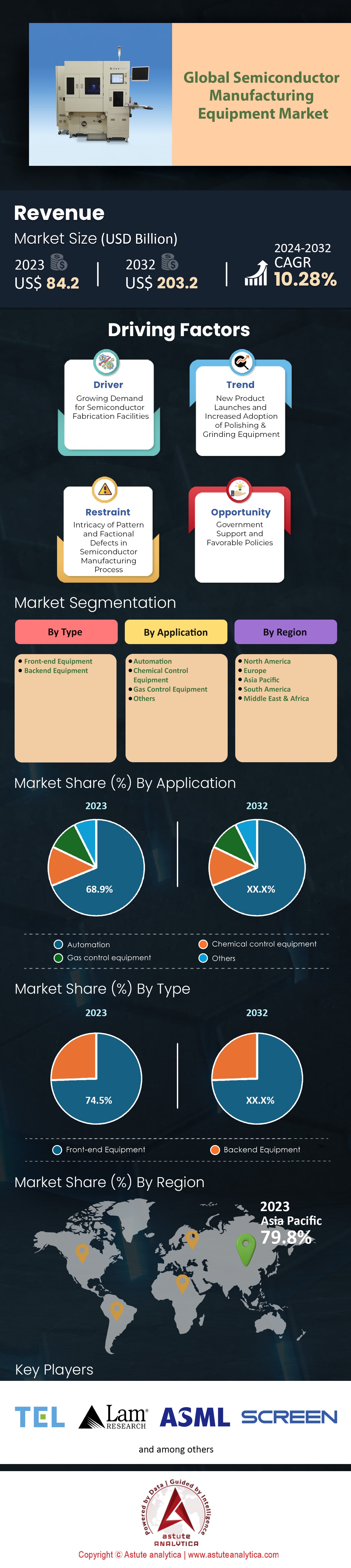
Semiconductor manufacturing equipment market was valued at US$ 93.03 billion in 2024 and is projected to attain a valuation of US$ 224.44 billion by 2033 at a CAGR of 10.28% during the forecast period 2025–2033.
Key Insights Shaping the Market
- Based on type, front-end equipment accounted for a dominant 74.5% of the total market revenue.
- On the application front, automation stands out as the most significant segment within the semiconductor manufacturing equipment market by capturing over 68.90% market share.
- Asia Pacific takes the lead in market and is set to remain the dominant one in the coming years.
A powerful wave of capital spending is redefining the semiconductor manufacturing equipment landscape, as orders are increasingly driven by record investments in AI and high-performance computing. For instance, overall global fab equipment spending is set to reach US$ 110 billion in 2025. Foundries are leading this charge with planned expenditures of approximately US$ 61 billion, alongside a robust US$ 37 billion from the memory sector. Consequently, this direct investment translates into significant orders, with foundry and logic equipment sales projected to hit US$ 64.8 billion. Furthermore, total sales for the entire semiconductor manufacturing equipment market are forecast to reach an unprecedented US$ 125.5 billion in 2025.
Specific technology bottlenecks, meanwhile, are creating highly concentrated demand across the ecosystem. In advanced packaging, for example, TSMC's CoWoS capacity is projected to surge to 80,000 wafers per month in 2025 from around 40,000 in 2024 to meet overwhelming customer need. Moreover, the critical dependency on EUV lithography for advanced nodes is also a major factor; ASML recorded a remarkable €5.4 billion in net bookings in its third quarter of 2025, with €3.6 billion of that dedicated to EUV systems. Simultaneously, back-end equipment is seeing a surge, with test equipment sales expected to reach a record US$ 9.3 billion while assembly and packaging tools climb to US$ 5.4 billion.
Geopolitical strategies are also actively reshaping demand flows across the global semiconductor manufacturing equipment market. Government-led initiatives like the U.S. CHIPS Act, which has allocated over US$ 33 billion in manufacturing grants, are creating new regional investment hubs. In parallel, China’s push for self-sufficiency is fueling massive growth for domestic suppliers, as evidenced by Naura Technology Group’s revenue expanding to ¥29.8 billion. However, this has created a bifurcated market where AI-related spending soars while other segments show caution. Illustrating this point, Samsung has cut its 2025 foundry capex to US$ 3.5 billion, while Intel's investment is projected to be around US$ 20 billion.
To Get more Insights, Request A Free Sample
New Frontiers in Equipment Demand Create Unprecedented Market Growth Opportunities
The semiconductor manufacturing equipment market is expanding into new, high-value technological domains. These emerging areas present significant growth opportunities for specialized equipment suppliers capable of meeting novel manufacturing challenges.
- The global transition to electric vehicles and advanced power grids is fueling a surge in demand for wide-bandgap semiconductors like Silicon Carbide (SiC) and Gallium Nitride (GaN). Manufacturing these materials requires highly specialized equipment for processes such as high-temperature crystal growth and epitaxial deposition. Consequently, equipment makers are seeing a new wave of orders for tools tailored specifically for the power semiconductor market, representing a lucrative and rapidly growing vertical.
- Furthermore, the semiconductor manufacturing equipment market’s shift toward chiplet-based designs and 3D stacking creates a critical need for next-generation metrology and inspection equipment. Ensuring the quality and reliability of thousands of micro-level connections between stacked dies requires tools with unprecedented precision. Therefore, companies providing advanced optical and e-beam inspection systems for detecting defects in die-to-wafer and wafer-to-wafer bonding are poised for substantial growth, as their technology becomes essential for enabling complex, high-performance computing systems.
High-Bandwidth Memory Expansion Creates Intense Demand for Specialized Back-End Tools
The production ramp-up for High-Bandwidth Memory (HBM) is a primary driver of investment in the semiconductor manufacturing equipment market. Memory makers are aggressively expanding capacity to meet AI-driven demand. For example, SK Hynix plans to invest over 14.6 trillion won in its next-generation HBM production lines. In addition, Samsung is aiming to triple its HBM output by the end of 2025. Micron has also committed over 1.2 trillion won to its HBM development facilities in Boise.
This expansion creates immense demand for specific back-end tools. Lead times for critical thermo-compression bonders have now extended to over 10 months. Each advanced bonder unit can cost between 3 billion and 5 billion won. The complexity is also increasing, with next-generation HBM4 moving to 16-layer stacks, requiring even greater precision. Consequently, equipment suppliers like Hanmi Semiconductor secured a landmark 150 billion won order for HBM manufacturing tools. Moreover, BES has received orders for over 2,200 of its advanced HBM reflow machines, and ASML is shipping 10 new hybrid bonding systems in 2025 to support this ramp.
Global Fab Construction Boom Guarantees a Multi-Year Equipment Order Pipeline in the Semiconductor Manufacturing Equipment Market
A worldwide push to regionalize chip production has ignited a massive fab construction cycle. Governments are providing substantial funding to secure domestic supply chains. For instance, Intel is moving forward with its massive €33 billion wafer fab complex in Magdeburg, Germany. In the U.S., TSMC has expanded its total investment commitment for its Arizona fabs to $65 billion. The U.S. CHIPS Act is directly fueling these projects, with GlobalFoundries receiving a $1.5 billion grant for its new and upgraded facilities.
These enormous projects translate directly into equipment orders. The cost of a single new leading-edge fab now exceeds $25 billion. These facilities across the semiconductor manufacturing equipment market are immense; TSMC’s Arizona site alone will contain two cleanrooms totaling over 600,000 square feet. Japan is also investing heavily, providing an initial subsidy of ¥590 billion for Rapidus’s new 2nm fab. In total, construction is starting on 35 new fabs globally between 2024 and 2025. Each new fab requires thousands of individual manufacturing tools. Furthermore, a facility like Intel’s Ohio One site will need 7,000 construction workers and over 3,000 permanent high-tech jobs, illustrating the scale of these operations.
Segmental Analysis
By Type: Front-End's Financial Might Forging Tomorrow's Powerful Microchips
Front-end equipment’s commanding 74.5% revenue share of the semiconductor manufacturing equipment market arises from its foundational role in semiconductor fabrication. These highly complex systems perform the most critical and capital‑intensive steps of chip creation on silicon wafers, including lithography, etching, and deposition—processes that define semiconductor performance. The immense cost of such machinery, with a single EUV lithography unit exceeding $200 million, anchors its market value. Building a state‑of‑the‑art fabrication plant demands investments of tens of billions of dollars, much of it devoted to front‑end tools. Major capital infusions, such as the U.S. government’s $50 billion initiative and ASML’s €5.1 billion raise in May 2025, highlight the segment’s financial gravity. The transition to 2 nm, 3 nm, and 4 nm nodes multiplies process complexity, reinforcing front‑end dominance in the semiconductor manufacturing equipment market.
Historic investment is driven by the rising technical demands of advanced chipmaking. Lam Research’s $1 billion facility in India (February 2025) and China’s domestic equipment funding exceeding ¥13 billion in 2025 exemplify this surge. Fabricating ≤5 nm chips can require up to four separate EUV exposures per layer, doubling lithography and multiplying etch, clean, and metrology steps. Spending in early 2025 reached $7.69 billion in Korea and $7.09 billion in Taiwan, underscoring massive front‑end focus worldwide. TSMC’s joint fab in Japan began pilot production in January 2025, with CMP ensuring a uniform wafer surface and oxidation forming crucial silicon dioxide insulation.
Customize This Report + Validate with an Expert
Access only the sections you need—region-specific, company-level, or by use-case.
Includes a free consultation with a domain expert to help guide your decision.
By Application: Automation Commands the Semiconductor Floor
When it comes to application, automation dominates semiconductor manufacturing equipment market, seizing a 68.90% market share. Its rise stems from the non‑negotiable demand for precision, uniformity, and contamination control—impossible to sustain manually. Automation minimizes human touchpoints, sharply reducing particles and defects that could nullify production. North American firms ordered 17,635 robots valued at $1.094 billion in H1 2025 alone, spanning robotic handlers to integrated control systems orchestrating entire production flows. Automation stretches beyond defect control—it enables a tenfold gain in chip value within smart‑factory settings.
The pursuit of throughput and operational efficiency keeps automation indispensable in the semiconductor manufacturing equipment market. In Q2 2025, 8,571 robot orders worth $513 million exemplified sustained momentum. Collaborative robots (“cobots”) represented 3,085 units in H1 2025, designed to partner safely with human technicians on precision‑critical tasks. Automation not only offsets the U.S. manufacturing talent gap—projected at 2.1 million by 2030—but ensures scalability of semiconductor output. AI‑driven predictive maintenance enhances production efficiency by pre‑empting downtime and improving yields, positioning smart systems as the backbone of competitive chip fabrication.
By 2035, fully automated “lights‑out” fabs are expected to become standard practice in the semiconductor manufacturing equipment market. Manufacturing Execution Systems (MES) will continuously supervise production in real time, coordinating extended toolchains from deposition to testing. Automated Test Equipment (ATE) ensures rapid, high‑volume assessment of semiconductor devices with unmatched accuracy, securing quality before shipment. Together, front‑end investment and automation form the dual financial engines propelling the Semiconductor Manufacturing Equipment Market into its next era of technological supremacy.
To Understand More About this Research: Request A Free Sample
Regional Analysis
Asia Pacific Commands Global Equipment Spending With Unmatched Fab Investment
The Asia Pacific region solidifies its position as the epicenter of the global semiconductor manufacturing equipment market. The scale of investment is monumental, led by China, which is projected to spend over $30 billion on fab equipment in 2025 alone. Taiwan remains a critical hub, with TSMC planning to invest between $28 billion and $32 billion in capital expenditures in 2024. Furthermore, TSMC’s advanced 2nm fab in Kaohsiung is expected to cost approximately $15.7 billion. In South Korea, Samsung is developing a massive new semiconductor cluster in Yongin, a project with a total planned investment of 300 trillion won.
The regional momentum extends beyond the giants in semiconductor manufacturing equipment market. Japan is re-emerging as a key player, with the government providing a ¥590 billion subsidy to support Rapidus’s new 2nm fab development. Additionally, TSMC is building its second Japanese fab in Kumamoto, with a total investment reaching over $20 billion for both facilities. South Korea’s SK Hynix is also investing a significant 14.6 trillion won into its next-generation HBM production. In Singapore, GlobalFoundries has committed to a $4 billion fab expansion. Lastly, China’s largest chipmaker, SMIC, is moving forward with four new fabs, with a combined investment value exceeding $20 billion.
North America Spearheads Supply Chain Reshoring With Massive Government Backing
North America semiconductor manufacturing equipment market is aggressively expanding its domestic chip manufacturing capabilities in the semiconductor manufacturing equipment market, driven by substantial government and private sector investment. The U.S. CHIPS and Science Act is a key catalyst, providing a direct grant of $8.5 billion to Intel for its advanced projects. Moreover, Intel is proceeding with its massive $20 billion dual-fab project in Ohio. TSMC has also increased its total investment commitment for its Arizona facilities to $65 billion. Similarly, Samsung is building a new advanced logic fab in Taylor, Texas, with an investment exceeding $17 billion.
The scale of these projects in the regional semiconductor manufacturing equipment market is creating a robust order pipeline for equipment suppliers. Micron is investing up to $100 billion over two decades for its new megafab in Clay, New York. Furthermore, GlobalFoundries received a $1.5 billion grant to expand its New York fab and build a new facility. In addition, Texas Instruments has begun construction on its new $11 billion fab in Lehi, Utah. The U.S. Commerce Department also awarded a $1.6 billion grant to SkyWater Technology. Finally, a new National Semiconductor Technology Center is being established with a budget of $5 billion to foster R&D.
Europe Strategically Invests to Reclaim Its Semiconductor Manufacturing Footprint
Europe semiconductor manufacturing equipment market is making a concerted effort to bolster its semiconductor ecosystem through targeted, large-scale investments under the European Chips Act framework. Germany is a central focus of activity, with Intel’s planned Magdeburg fab complex representing a monumental €33 billion investment. Additionally, Wolfspeed is constructing a new 200mm SiC device fab in Saarland, Germany, with an initial cost of $3 billion. The European Commission also approved a significant €902 million in state aid for Northvolt's battery and semiconductor facility.
The investment strategy extends across the continent. In France, STMicroelectronics and GlobalFoundries are jointly building a new high-volume semiconductor manufacturing facility in Crolles with a total investment of €7.5 billion. The Irish government also approved a €5 billion investment for Intel’s Fab 34 expansion project in Leixlip. Furthermore, the leading European research hub, Imec, is set to receive €2.5 billion to build a new pilot line for sub-2nm process development. The European Chips Act itself aims to mobilize over €43 billion in public and private investments, creating a strong, long-term demand signal for equipment suppliers.
Recent Developments in Semiconductor Manufacturing Equipment Market
- Edwards Vacuum, a critical supplier, announced investment to build a new manufacturing facility in South Korea for integrated vacuum and abatement systems.
- Chinese equipment maker Naura Technology Group raised funds in early 2025 to fund strategic acquisitions, including a controlling stake in Kingsemi.
- Photonics and laser system provider MKS Instruments acquired Atotech for $4.4 billion to expand its portfolio for advanced electronics manufacturing.
- Semiconductor materials supplier Entegris acquired CMC Materials for $5.7 billion to create a comprehensive electronic materials platform for the industry.
- China's state-backed "Big Fund III" was officially established with a registered capital of 344 billion yuan ($47.5 billion) to invest in domestic equipment and material firms.
Top Players in the Global Semiconductor Manufacturing Equipment Market
- Tokyo Electron Limited
- Lam Research Corporation
- Asml Holdings N.V.
- KLA-Tencor Corporation
- Screen Holdings Co., Ltd.
- Applied Materials Inc.
- Teradyne Inc.
- Hitachi High-Technologies Corporation
- Plasma-Therm
- Rudolph Technologies, Inc
- Advantest Corporation
- Startup Ecosystem
- Other Prominent Players
Market Segmentation Overview:
By Type
- Front-end Equipment
- Backend Equipment
By Application
- Automation
- Chemical Control Equipment
- Gas Control Equipment
- Others
By Region
- North America
- The U.S.
- Canada
- Mexico
- Europe
- Western Europe
- The UK
- Germany
- France
- Italy
- Spain
- Rest of Western Europe
- Eastern Europe
- Poland
- Russia
- Rest of Eastern Europe
- Western Europe
- Asia Pacific
- China
- India
- Japan
- Australia & New Zealand
- ASEAN
- Rest of Asia Pacific
- Middle East & Africa (MEA)
- UAE
- Saudi Arabia
- South Africa
- Rest of MEA
- South America
- Argentina
- Brazil
- Rest of South America
LOOKING FOR COMPREHENSIVE MARKET KNOWLEDGE? ENGAGE OUR EXPERT SPECIALISTS.
SPEAK TO AN ANALYST
.svg)


Features | Type of License | ||||
Data Book | Single User |   Multi User | Corporate | ||
| e-Access | ✓ | ✓ | ✓ | ✓ | |
User Sharing | 1 User Only | 1 User Only | Up to 7 Users | Unlimited User Access | |
⨉ | ⨉ | ⨉ | ✓ | ||
Free Customization | No Free Customization | Up To 30 hrs work | Up To 60 hrs work | Up To 80 hrs work | |
Deliverable |
| ⨉ | ✓ | ✓ | ✓ |
| ✓ | ⨉ | ✓ | ✓ | |
| ⨉ | ⨉ | ⨉ | ✓ | |
Analyst Support | 2-Months Analyst Support | 4-Months Analyst Support | 7-Months Analyst Support | One Year Analyst Support | |
Free Report update in next update cycle | ⨉ | ⨉ | ⨉ | ✓ | |
Free Industry Update (Within 180 days) | ⨉ | ⨉ | ⨉ | ✓ | |
Benefit | Up to 10% off on Post Purchase | Up to 20% off on Post Purchase | Up to 30% off on Post Purchase | Up to 40% off on Post Purchase | |