Thin-Film Lithium Niobate Devices Market: Product Type (TFLN Wafers, TFLN Photonic Chips, Integrated TFLN PICs (Photonic Integrated Circuits), TFLN Optical Subassemblies, TFLN Development Kits & Prototyping Boards); Cut Type (X-Cut, Y-Cut, Z-Cut, Custom Orientation); Thickness (Upto 300 nm, 300-600 nm, Above 600 nm); Device Type (Electro-Optic Modulators, Switches, Frequency Converters / Nonlinear Optical Devices, Filters and Resonators, LiDAR Transmitters (Photonic Sources + Modulators), RF Photonics Components, Quantum Photonics Devices, Test and Measurement Modules); Deposition Method (Smart-Cut/ION Slicing, Epitaxial Growth, Bonding and Layer Transfer Techniques, Others); Substrate Material (Silicon Substrates, Sapphire Substrates, Lithium Tantalate Substrates, Others); Material Type (Thin Film Lithium Niobate, Hybrid Materials); Application (Telecommunications, Healthcare, Automotive, Industrial Automation, Research and Development, Others); Distribution Channel (Direct, Distributors, Online); Region—Market Size, Industry Dynamics, Opportunity Analysis and Forecast for 2025–2033
- Last Updated: 05-Jul-2025 | | Report ID: AA07251368
Market Scenario
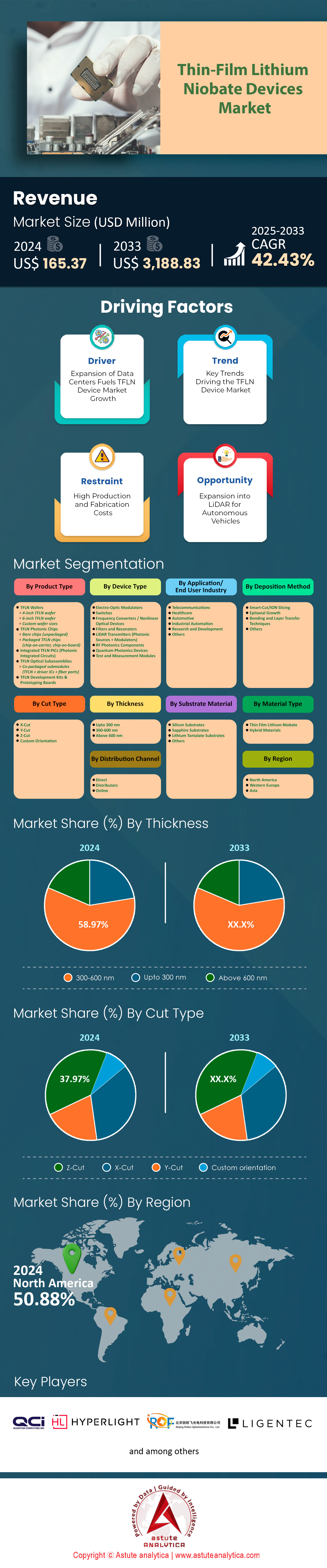
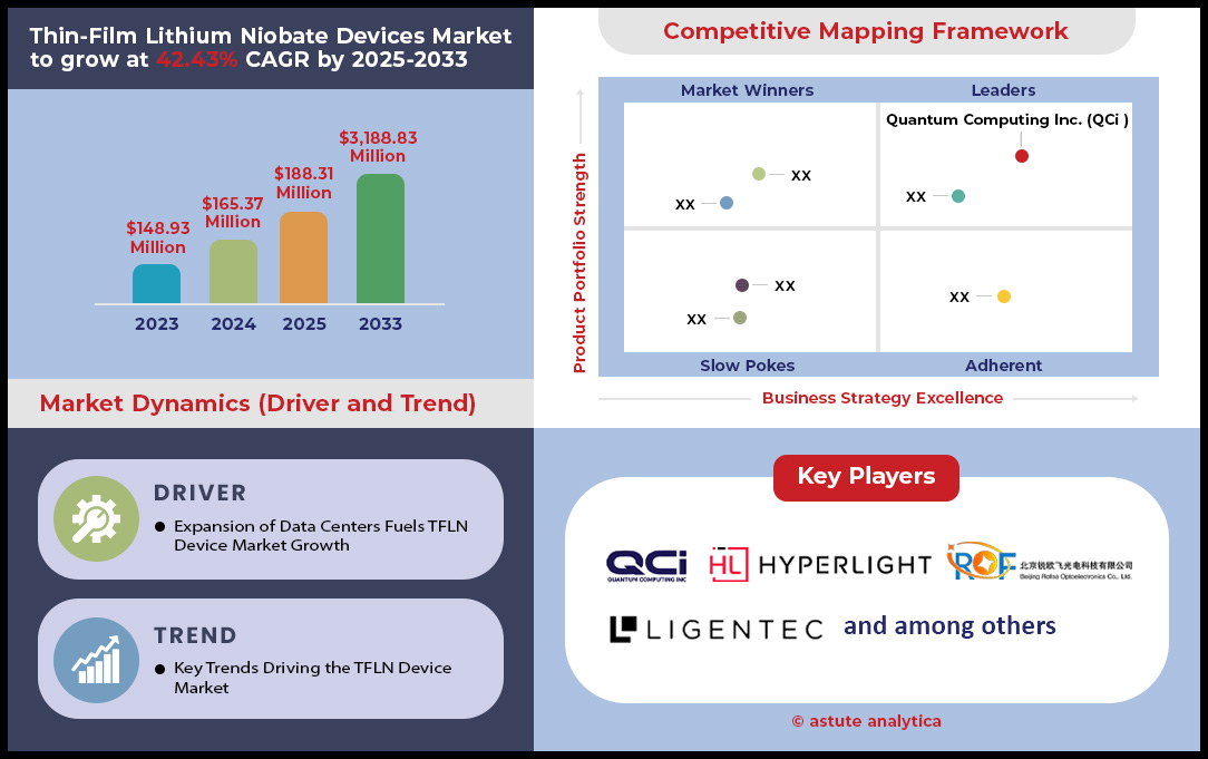
Thin-film lithium niobate devices market was valued at US$ 165.37 million in 2024 and is projected to hit the market valuation of US$ 3,188.83 million by 2033 at a CAGR of 42.43% during the forecast period 2025–2033.
The thin-film lithium niobate (TFLN) devices market is experiencing a surge in demand across several high-growth sectors, each presenting unique opportunities for market stakeholders. In telecommunications, the global rollout of 5G networks and the insatiable appetite for high-speed, high-bandwidth data transmission are propelling the adoption of advanced photonic components. TFLN devices, with their superior performance characteristics, are increasingly being integrated into next-generation optical networks, making them a strategic focus for telecom equipment manufacturers and network operators. Meanwhile, the quantum technology sector is rapidly evolving, with TFLN devices being explored for quantum photonics applications. The push for miniaturization and integration in quantum devices is creating a demand for scalable, manufacturable TFLN solutions, positioning them as a key enabling technology for future quantum hardware.
The automotive industry in the Thin-film lithium niobate devices market is also undergoing a transformation, driven by the shift toward electric vehicles (EVs) and autonomous driving. This evolution is increasing the need for advanced sensors and communication modules, with TFLN devices being considered for vehicle-to-everything (V2X) communications and high-performance sensing. These trends align with the automotive sector’s move toward smart, connected vehicles. Additionally, regulatory and societal pressures for real-time, accurate environmental data are boosting demand for advanced sensor technologies. TFLN-based sensors are being adopted for air and water quality monitoring, as well as radiation detection, supporting compliance and sustainability initiatives. Collectively, these industry-specific trends underscore the broad and growing relevance of TFLN devices, offering stakeholders multiple avenues for strategic investment and market expansion.
Key Insights in Thin-Film Lithium Niobate Devices Market
| Area | Key Insight |
| Industry Trends | 5G, quantum, automotive, and environmental sectors driving demand for TFLN devices |
| Regulatory Environment | Compliance with telecom, environmental, and IP regulations is essential |
| Supply Chain | Secure sourcing, scalable manufacturing, and resilient logistics are critical |
| Competitive Landscape | Dominated by innovation-driven, globally active companies |
| Adoption Barriers | High initial costs, workforce gaps, regulatory complexity, and organizational inertia |
| Strategic Opportunities | Integration, sustainability, global reach, and partnerships |
To Get more Insights, Request A Free Sample
Navigating Regulatory, Environmental, and Intellectual Property Challenges in Thin-Film Lithium Niobate Devices Market
The regulatory and policy environment surrounding TFLN devices is complex and multifaceted, requiring careful navigation by market stakeholders. In the telecommunications sector, the adoption of TFLN devices is heavily influenced by compliance with standards set by regulatory bodies such as the FCC in the United States and ETSI in Europe. Ensuring that products meet these regulatory requirements is essential for accessing key markets and avoiding costly delays or penalties. Environmental compliance is another critical consideration, as the manufacturing and disposal of TFLN devices are subject to regulations like the EU’s RoHS directive, which restricts the use of hazardous substances. Adhering to these standards is not only necessary for market access but also enhances brand reputation and consumer trust.
Intellectual property (IP) and trade policies play a significant role in shaping the competitive landscape of the Thin-film lithium niobate devices market. The industry is highly IP-intensive, with patents serving as a cornerstone of competitive positioning. Trade policies and international agreements can impact the import and export of TFLN materials and devices, influencing global supply chains and market reach. Regional policy support further shapes the industry’s trajectory; for example, Asian countries such as China and Japan are actively supporting advanced materials industries through government funding and favorable policies, while the United States emphasizes innovation incentives and competitive practices. Stakeholders must remain vigilant to regional policy shifts, as these can present both strategic opportunities and potential barriers to entry. Proactive engagement with regulatory frameworks and policy developments is thus essential for sustained success in the TFLN market.
Building Resilient Supply Chains and Scalable Manufacturing for TFLN Device Success Set to Change the Market Momentum
Supply chain and manufacturing dynamics are central to the commercial success of Thin-film lithium niobate devices market, demanding strategic attention from market stakeholders. The availability of raw materials—specifically lithium and niobium, the core elements for TFLN—is subject to geopolitical and regulatory influences. Ensuring secure, ethical, and sustainable sourcing is increasingly important, both for risk mitigation and for meeting growing expectations around corporate responsibility. As demand for TFLN devices rises, scaling up production to meet market needs becomes a key challenge. This requires significant investment in advanced manufacturing infrastructure and process optimization to ensure cost-effective, high-volume output without compromising quality.
Quality assurance and reliability are paramount, especially in sectors such as telecommunications and automotive, where device failure can have significant consequences in the Thin-film lithium niobate devices market. Maintaining high standards throughout the manufacturing process is essential for market acceptance and long-term customer relationships. Efficient, global distribution networks are also necessary to serve the diverse range of sectors adopting TFLN technology. Effective logistics management and inventory control are vital for timely delivery and customer satisfaction. Recent global disruptions, such as the COVID-19 pandemic, have underscored the importance of supply chain resilience. Diversification of suppliers and the adoption of digital supply chain management tools are becoming best practices, enabling companies to respond swiftly to unforeseen challenges and maintain business continuity.
Innovation, Partnerships, and Global Reach Define the Competitive TFLN Landscape
The competitive landscape of the Thin-film lithium niobate devices market is characterized by innovation-driven, globally active companies that are shaping the future of photonics and advanced materials. Key players such as HyperLight, SRICO, Photonic Systems, Advanced Fiber Resources, Eoptolink Technology, Tianjin H-Chip Technology Group, Stanford Advanced Materials, American Elements, and Merck are at the forefront, differentiating themselves through technological innovation, manufacturing scale, and global reach. These companies invest heavily in research and development (R&D) to maintain technological leadership and secure intellectual property, which serves as a critical competitive advantage in this rapidly evolving sector.
Strategic partnerships are a hallmark of the industry, with collaborations between TFLN device manufacturers and system integrators—such as telecom equipment vendors and automotive original equipment manufacturers (OEMs)—accelerating product development and market entry. These alliances in the Thin-film lithium niobate devices market enable companies to leverage complementary strengths, reduce time-to-market, and address complex customer requirements more effectively. The focus on R&D not only drives innovation but also helps companies stay ahead of regulatory changes and emerging market trends. As the industry continues to mature, the ability to form strategic partnerships, invest in cutting-edge research, and expand global operations will be key differentiators for companies seeking to establish and maintain leadership in the TFLN market.
Overcoming Adoption Barriers: Investment, Workforce, and Regulatory Complexity in TFLN
Despite the promising outlook for Thin-film lithium niobate devices market, market stakeholders must contend with several adoption challenges and barriers that can impact the pace and scale of industry growth. One of the most significant hurdles is the high initial investment required for adopting TFLN technology. This includes substantial upfront costs for equipment, infrastructure, and workforce training, necessitating a careful assessment of return on investment (ROI) and long-term cost-effectiveness. Additionally, there is a notable shortage of skilled labor with expertise in TFLN device manufacturing and integration. Addressing this gap requires targeted investment in training and talent development to build a workforce capable of supporting advanced manufacturing processes.
Regulatory and standards compliance presents another layer of complexity for the Thin-film lithium niobate devices market growth, as navigating the intricate and evolving landscape of regulations can delay product launches and increase operational costs. Early engagement with regulatory bodies and standards organizations is recommended to streamline compliance and minimize disruptions. Organizational resistance to change is also a common barrier, particularly in established industries with legacy systems. Effective change management strategies are essential to overcome internal inertia and facilitate the successful adoption of new technologies. By proactively addressing these challenges—through investment, workforce development, regulatory engagement, and organizational change—stakeholders can position themselves to capitalize on the significant opportunities presented by the TFLN device market.
Strategic Opportunities: Integration, Sustainability, and Global Expansion in TFLN Markets
The Thin-film lithium niobate devices market offers a wealth of strategic opportunities for market stakeholders willing to invest in integration, sustainability, and global expansion. The trend toward integrating multiple functionalities into compact devices is creating new avenues for TFLN-based solutions across a variety of sectors, from telecommunications and quantum computing to automotive and environmental monitoring. Companies that prioritize sustainable sourcing and manufacturing practices can enhance their environmental, social, and governance (ESG) profiles, which is increasingly important to investors and customers alike. Emphasizing sustainability not only supports regulatory compliance but also strengthens brand reputation and market differentiation.
Global expansion is another critical opportunity, as the adoption of Thin-film lithium niobate devices market continues to grow worldwide. Companies with robust international distribution and compliance capabilities are better positioned to capture emerging market opportunities and respond to regional policy shifts. Forming technological partnerships with research institutions and technology partners can accelerate innovation and reduce time-to-market for new TFLN-based products. These alliances enable companies to access cutting-edge research, share resources, and navigate complex regulatory environments more effectively. By focusing on integration, sustainability, global reach, and strategic partnerships, market stakeholders can unlock the full potential of the TFLN device industry and secure a competitive edge in this dynamic and rapidly evolving market.
Segmental Analysis
By Product Type
TFLN wafers dominate the thin-film lithium niobate devices market by capturing over 34.55% market share due to their fundamental role as the substrate platform for nearly all advanced photonic applications. These wafers serve as the essential starting material for fabricating integrated photonic circuits, modulators, and quantum devices. Major telecommunications equipment manufacturers like Huawei and Nokia rely on TFLN wafers to produce high-performance optical components for their 5G infrastructure deployments. The wafers enable monolithic integration of multiple photonic functions on a single chip, significantly reducing device footprint and improving performance. For instance, a single 4-inch TFLN wafer can yield over 1,000 individual modulator chips, making it highly cost-effective for mass production. The superior electro-optic coefficient of lithium niobate (r33 = 30.8 pm/V) combined with the thin-film format allows for unprecedented modulation efficiency and bandwidth capabilities exceeding 100 GHz.
The dominance of TFLN wafers in the thin-film lithium niobate devices market is further reinforced by their versatility across diverse applications. Data centers operated by companies like Google and Amazon Web Services increasingly adopt TFLN-based components for their optical interconnects, driving wafer demand. The wafers support various device architectures including Mach-Zehnder modulators, ring resonators, and directional couplers, all fabricated using standard semiconductor processes. Manufacturing advances have enabled wafer sizes up to 6 inches in diameter with thickness uniformity better than ±5 nm across the entire surface. This precision is critical for maintaining consistent device performance in high-volume production. The ability to produce TFLN wafers through the Smart-cut process, which involves ion implantation, wafer bonding, and chemical-mechanical polishing, has reduced production costs by approximately 40% over the past five years, making them more accessible to emerging market segments.
By Cut Type
Z-cut lithium niobate dominates the thin-film lithium niobate devices market with nearly 38% share because it offers the most efficient utilization of the material's largest electro-optic coefficient (r33). In Z-cut orientation, the electric field applied perpendicular to the crystal surface directly interacts with the r33 coefficient, resulting in maximum phase modulation efficiency. This configuration is particularly advantageous for telecommunications applications where Vπ (the voltage required for π phase shift) needs to be minimized. For example, commercial Z-cut TFLN modulators achieve Vπ values as low as 1.2 V for a 1-cm device length, compared to 3-4 V for X-cut or Y-cut orientations. Major optical transceiver manufacturers like Lumentum and II-VI Incorporated specifically design their products around Z-cut TFLN to meet stringent power consumption requirements in data centers, where each milliwatt saved translates to significant operational cost reductions.
The preference for Z-cut in the thin-film lithium niobate devices market extends beyond telecommunications to quantum photonics and sensing applications. In quantum computing systems developed by companies like IonQ and Rigetti, Z-cut TFLN devices enable precise manipulation of quantum states with minimal crosstalk. The orientation provides superior temperature stability with a temperature coefficient of refractive index (dn/dT) of 4×10⁻⁵/°C, crucial for maintaining phase matching in nonlinear optical processes. Z-cut TFLN is predominantly used in high-speed electro-optic modulators for coherent optical communications, achieving data rates exceeding 800 Gb/s per wavelength. Additionally, aerospace companies utilize Z-cut TFLN in fiber optic gyroscopes for navigation systems, where the orientation's stability and low acoustic noise characteristics are essential. The fabrication yield for Z-cut devices is approximately 15% higher than X-cut or Y-cut alternatives due to reduced stress-induced defects during the thin-film transfer process.
By Device Type
Electro-optic modulators lead the thin-film lithium niobate devices market with over 39.51% share due to the explosive growth in data center interconnects and 5G infrastructure deployments. These devices convert electrical signals to optical signals with unprecedented efficiency, achieving modulation rates exceeding 100 Gb/s per channel while consuming less than 1 pJ/bit of energy. Major cloud service providers including Microsoft Azure and Alibaba Cloud have deployed TFLN modulators in their data centers to support bandwidth-intensive applications like artificial intelligence training and real-time video streaming. The global data center IP traffic, which reached 20.6 zettabytes in 2024, drives continuous demand for higher-capacity optical interconnects. TFLN modulators enable 400G and 800G Ethernet standards with a single device, compared to the multiple discrete components required by traditional lithium niobate or silicon photonic solutions. Companies like Marvell and Broadcom have invested over US$ 500 million collectively in TFLN modulator development for next-generation optical transceivers.
The dominance of electro-optic modulators in the thin-film lithium niobate devices market reflects their versatility across emerging applications beyond traditional telecommunications. In 5G networks, TFLN modulators enable analog radio-over-fiber links with spurious-free dynamic ranges exceeding 110 dB·Hz²/³, critical for distributed antenna systems in urban deployments. Quantum communication systems utilize TFLN modulators for quantum key distribution, achieving secure key rates above 10 Mb/s over 100-km fiber links. The automotive LiDAR market, projected to reach US$ 8.5 billion by 2030, increasingly adopts TFLN modulators for beam steering and frequency modulation. Defense contractors like Lockheed Martin and Raytheon integrate TFLN modulators in electronic warfare systems for ultra-wideband signal processing. Key end-use applications include coherent optical transceivers (45% of demand), microwave photonic links (25%), quantum photonics (15%), and sensing systems (15%). The concentration of demand from hyperscale data centers in North America and Asia-Pacific regions, which account for over 70% of global data center capacity, ensures continued growth for TFLN electro-optic modulators.
By Thickness
The 300-600 nm thickness range dominates the thin-film lithium niobate devices market with over 59% share because it represents the optimal balance between optical confinement, modulation efficiency, and manufacturing yield At these thicknesses, the optical mode is tightly confined within the lithium niobate layer, enabling strong light-matter interaction while maintaining single-mode operation at telecommunications wavelengths (1,310-1,550 nm). For instance, a 400-nm thick TFLN waveguide achieves an effective index contrast of 0.7 with silicon dioxide cladding, resulting in bend radii as small as 50 μm without significant radiation loss. This tight confinement allows device footprints to be reduced by a factor of 100 compared to bulk lithium niobate devices. Major foundries like LIGENTEC and HyperLight have standardized their processes around the 300-600 nm range, achieving propagation losses below 0.1 dB/cm and coupling efficiencies exceeding 90% with standard optical fibers.
The demand for 300-600 nm thickness in the thin-film lithium niobate devices market is driven by specific performance requirements across multiple applications In high-speed modulators, this thickness range enables electrode gaps of 5-10 μm while maintaining excellent mode overlap with the applied electric field, resulting in modulation bandwidths exceeding 110 GHz. Quantum photonics applications benefit from the reduced mode volume, which enhances nonlinear optical processes – for example, second-harmonic generation efficiency improves by a factor of 1,000 compared to bulk devices. The 300-600 nm range also facilitates heterogeneous integration with silicon photonics platforms, as demonstrated by Intel's co-packaged optics solutions. Manufacturing data shows that wafers with 300-600 nm thickness achieve defect densities below 0.5 defects/cm², compared to 5-10 defects/cm² for thicker films. This superior quality translates to device yields exceeding 85% for commercial production runs, making this thickness range the most economically viable for high-volume manufacturing.
Customize This Report + Validate with an Expert
Access only the sections you need—region-specific, company-level, or by use-case.
Includes a free consultation with a domain expert to help guide your decision.
To Understand More About this Research: Request A Free Sample
Regional Analysis
North America Leads Through Advanced R&D and Infrastructure Investments
North America commands over 50.88% of the global thin-film lithium niobate devices market, driven by its unparalleled concentration of research institutions, data centers, and telecommunications infrastructure. The region hosts over 2,800 data centers, with hyperscale facilities operated by Amazon Web Services, Microsoft Azure, and Google Cloud Platform actively integrating TFLN-based optical interconnects for enhanced performance. Major telecommunications equipment manufacturers including Lumentum Operations and II-VI Incorporated have established specialized TFLN fabrication facilities across the region, collectively investing over US$ 1.2 billion in advanced photonics infrastructure since 2022. The presence of leading research universities such as MIT, Stanford, and Caltech creates a robust innovation ecosystem, with these institutions collectively filing over 85 patents related to TFLN applications in 2024 alone. Furthermore, the region's mature venture capital ecosystem has funded 47 TFLN-focused startups with total investments exceeding US$ 680 million, accelerating commercialization of cutting-edge applications from quantum computing to advanced sensing systems.
United States Drives Regional Growth Through Strategic Federal Investments
The United States serves as the primary engine of the thin-film lithium niobate devices market within North America, benefiting from strategic federal investments and a thriving technology sector. The Department of Defense has allocated US$ 450 million specifically for photonic integrated circuit development, with TFLN devices identified as critical components for secure communications and electronic warfare systems. Silicon Valley alone houses 23 companies developing TFLN-based products, ranging from quantum photonic processors to ultra-high-speed modulators for data center applications. The National Science Foundation's Quantum Leap Challenge Institutes have established dedicated TFLN research programs at five major universities, producing over 120 doctoral graduates specializing in this technology annually. American semiconductor foundries, including GlobalFoundries and SkyWater Technology, have developed specialized TFLN process flows, achieving production yields exceeding 85% for commercial devices. The convergence of federal support, private investment, and technical expertise has created an innovation flywheel effect, with US companies launching 34 new TFLN-based products in 2024, spanning applications from autonomous vehicle sensors to satellite communications.
Asia Pacific Emerges as Manufacturing Powerhouse and Growth Engine
Asia Pacific represents the second-largest regional thin-film lithium niobate devices market, leveraging its manufacturing excellence and rapidly expanding telecommunications infrastructure. The region's semiconductor foundries in Taiwan, Singapore, and South Korea have established dedicated TFLN production lines with combined monthly capacity exceeding 12,000 wafers, serving both domestic and international customers. China's aggressive 5G rollout, encompassing over 2.3 million base stations, creates substantial demand for TFLN-based modulators and filters, with domestic manufacturers like Huawei integrating these components into next-generation network equipment. Japan's precision manufacturing capabilities have enabled companies to achieve TFLN device specifications with tolerances below 10 nanometers, essential for quantum photonics applications. The region benefits from strong government support, with Singapore's Economic Development Board providing US$ 200 million in incentives for photonics manufacturing facilities, while South Korea's Ministry of Science and ICT has designated TFLN as a strategic technology with dedicated research funding of US$ 350 million through 2027.
Top Players in Thin-Film Lithium Niobate Devices Market
- HyperLight
- SRICO
- OneTouch Technology
- Beijing Rofea Optoelectronics
- Quantum Computing Inc. (QCi )
- Ori-Chip
- AFR
- Agiltron
- Thorlab
- Fujitsu
- Other Prominent Players
Market Segmentation Overview
By Product Type
- TFLN Wafers
- 4-inch TFLN wafer
- 6-inch TFLN wafer
- Custom wafer sizes
- TFLN Photonic Chips
- Bare chips (unpackaged)
- Packaged TFLN chips (chip-on-carrier, chip-on-board)
- Integrated TFLN PICs (Photonic Integrated Circuits)
- TFLN Optical Subassemblies
- Co-packaged submodules (TFLN + driver ICs + fiber ports)
- TFLN Development Kits & Prototyping Boards
By Cut Type
- X-Cut
- Y-Cut
- Z-Cut
- Custom Orientation
By Thickness
- Upto 300 nm
- 300-600 nm
- Above 600 nm
By Device Type
- Electro-Optic Modulators
- Switches
- Frequency Converters / Nonlinear Optical Devices
- Filters and Resonators
- LiDAR Transmitters (Photonic Sources + Modulators)
- RF Photonics Components
- Quantum Photonics Devices
- Test and Measurement Modules
By Deposition Method
- Smart-Cut/ION Slicing
- Epitaxial Growth
- Bonding and Layer Transfer Techniques
- Others
By Substrate Material
- Silicon Substrates
- Sapphire Substrates
- Lithium Tantalate Substrates
- Others
By Material Type
- Thin Film Lithium Niobate
- Hybrid Materials
By Application/End User Industry
- Telecommunications
- Healthcare
- Automotive
- Industrial Automation
- Research and Development
- Others
By Distribution Channel
- Direct
- Distributors
- Online
By Region
- North America
- The U.S.
- Canada
- Mexico
- Western Europe
- The UK
- Germany
- France
- Italy
- Spain
- Rest of Western Europe
- Asia Pacific
- China
- India
- Japan
- South Korea
- Australia & New Zealand
- ASEAN
- Rest of Asia Pacific
LOOKING FOR COMPREHENSIVE MARKET KNOWLEDGE? ENGAGE OUR EXPERT SPECIALISTS.
SPEAK TO AN ANALYST
.svg)


Features | Type of License | ||||
Data Book | Single User |   Multi User | Corporate | ||
| e-Access | ✓ | ✓ | ✓ | ✓ | |
User Sharing | 1 User Only | 1 User Only | Up to 7 Users | Unlimited User Access | |
⨉ | ⨉ | ⨉ | ✓ | ||
Free Customization | No Free Customization | Up To 30 hrs work | Up To 60 hrs work | Up To 80 hrs work | |
Deliverable |
| ⨉ | ✓ | ✓ | ✓ |
| ✓ | ⨉ | ✓ | ✓ | |
| ⨉ | ⨉ | ⨉ | ✓ | |
Analyst Support | 2-Months Analyst Support | 4-Months Analyst Support | 7-Months Analyst Support | One Year Analyst Support | |
Free Report update in next update cycle | ⨉ | ⨉ | ⨉ | ✓ | |
Free Industry Update (Within 180 days) | ⨉ | ⨉ | ⨉ | ✓ | |
Benefit | Up to 10% off on Post Purchase | Up to 20% off on Post Purchase | Up to 30% off on Post Purchase | Up to 40% off on Post Purchase | |