Wafer Dicing Services Market: By Material (Silicon Carbide, Alumina, Silicon, Others (Sapphire, Pyrex Glass, Glass, etc.)); Size (300 mm, 200 mm, Others); Dicing Technology (Wafer Scribing & Breaking, Mechanical Sawing, Laser Dicing, and Plasma Dicing); Region—Market Forecast and Analysis for 2026–2035
- Last Updated: 10-Dec-2025 | | Report ID: AA0723534
Market Snapshot
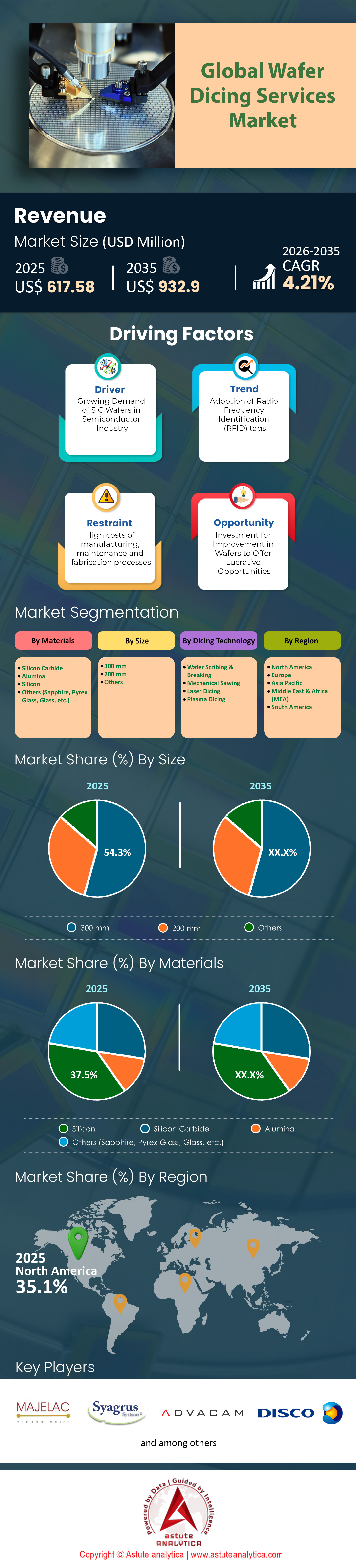
Wafer dicing services market was valued at US$ 617.5 million in 2025 and is projected to exceed valuation of US$ 932.9 million by 2035 at a CAGR of 4.21% during the forecast period 2026–2035.
Key Findings
- In terms of material, silicon carbide continues to be a dominant force in the market by accounted for over 37.5% of the market share.
- When it comes to size, the 300 nm segment dominates the market, accounting for over 54.3% of the market share.
- Based on dicing technology, the market is divided into Wafer Scribing & Breaking, Mechanical Sawing, Laser Dicing, and Plasma Dicing. Among these, laser dicing has emerged as the preferred dicing method, commanding over 42% of the market share.
- North is holding dominant position in the market by capturing over 35% market share.
The global semiconductor landscape is currently navigating a period of intense structural evolution, creating a robust and aggressive environment for the wafer dicing services market. The market is moving past the era where dicing was merely a commoditized final step in chip manufacturing. Today, it has become a critical value-add process that determines the yield and performance of high-end devices. The market is primarily headed by capacity tightness and urgent infrastructure scaling. With the semiconductor industry projected to reach new revenue heights, the backend processing sector is scrambling to keep pace with the front-end foundry output.
The demand is no longer cyclical but is being driven by a supercycle of artificial intelligence and electrification that requires continuous, high-volume throughput. Service providers are running production lines at near-maximum utilization rates, particularly for advanced nodes, as fabless companies and IDMs clamor for packaging slots that can handle fragile, high-performance materials. Consequently, the Wafer dicing services market is witnessing a valuation reset, where precision capability commands a significant premium over standard mechanical cutting.
To Get more Insights, Request A Free Sample
Which Prominent Product Types Are Witnessing Higher Demand Worldwide?
While mechanical blade dicing remains a workhorse for standard logic and consumer electronics, the most prominent product types currently witnessing explosive demand are laser ablation and stealth dicing technologies. Such a shift in the wafer dicing services market is necessitated by the physics of modern chip architecture. As wafers become thinner to accommodate 3D stacking, mechanical stress from saw blades causes unacceptable micro-cracks and yield losses. Stealth dicing, which creates a modification layer within the silicon using a laser before expanding the tape to separate dies, is becoming the standard for 300mm wafers used in memory and AI applications.
The method offers zero kerf width loss and cleaner side walls, which is essential when die real estate is incredibly expensive. Furthermore, plasma dicing is gaining traction for ultra-small dies where increasing the number of chips per wafer is paramount. The industry is effectively bifurcating, with premium value flowing heavily toward these non-contact, high-precision dicing methodologies that can navigate narrow streets and complex topographies without damaging active circuitry. Stakeholders in the Wafer dicing services market are increasingly retiring legacy saws in favor of these photonic solutions.
What Are the Primary Factors Fueling This Unprecedented Demand?
Two massive engines are fueling this unprecedented demand for the Wafer dicing services market. The first and most immediate factor is the Generative AI boom. AI accelerators, such as NVIDIA’s Blackwell architecture, rely heavily on High Bandwidth Memory (HBM). HBM production involves vertically stacking up to 12 or 16 ultra-thin dies, meaning a single sold unit represents a twelve-fold or sixteen-fold increase in dicing requirements compared to a standard planar chip. The precision required to dice these sub-50-micron layers without shattering them is driving a massive upgrade cycle in dicing equipment and service contracts.
A second major factor driving the wafer dicing services market growth is the automotive sector's transition to Silicon Carbide (SiC) for electric vehicles. SiC is notoriously hard and brittle, making it difficult to cut with traditional blades. As automakers push for 800V architectures, the volume of SiC wafers is skyrocketing, forcing service providers to adopt specialized laser solutions capable of processing these advanced materials efficiently.
Where Is the Global Demand Mainly Concentrated?
Geographically, the demand for the wafer dicing services market is overwhelmingly concentrated in the Asia-Pacific region. Such concentration is a direct result of the existing semiconductor supply chain ecosystem. Taiwan remains the absolute epicenter, serving as the primary hub for advanced packaging and foundry services that feed the global AI machinery. Proximity to major foundries like TSMC ensures that dicing services are integrated tightly into the "wafer-out" logistical flow. South Korea holds the second position of influence, driven almost exclusively by its dominance in the memory market and the HBM supply chain controlled by SK Hynix and Samsung.
However, the global wafer dicing services market is witnessing a strategic shift where demand is emerging in the United States and Japan. U.S. demand is being catalyzed by the CHIPS Act and the onshoring of advanced packaging facilities in Arizona and Texas, creating a nascent but rapidly growing need for domestic dicing capabilities to support secure supply chains for defense and critical infrastructure.
Who Are the Top Four Nations Dominating Production?
When analyzing the primary producers and hubs for dicing execution, four nations stand out as the pillars of the wafer dicing services market.
- Taiwan leads the pack, leveraging its massive OSAT (Outsourced Semiconductor Assembly and Test) infrastructure to handle the bulk of the world’s logic and AI silicon.
- South Korea is the undisputed leader in memory-related dicing, with its domestic output scaling in direct correlation to the insatiable global appetite for DRAM and NAND flash.
- China remains a volume heavyweight, particularly for legacy nodes, power management ICs, and the rapidly expanding domestic SiC sector intended for its massive EV market.
- Japan plays a unique dual role. It is not only a hub for high-precision dicing services for automotive sensors and power modules but also the home of the world’s leading dicing equipment manufacturers, making it the technological heart where new dicing processes are developed before being exported to the rest of the world.
Which Top Applications are Witnessing Rapid Adoption Lately?
Applications witnessing the most rapid adoption of specialized Wafer dicing services market solutions are High Bandwidth Memory (HBM) modules and automotive power inverters. In the HBM space, the transition to HBM3E and the upcoming HBM4 standard is the single largest volume driver. These memory stacks are essential for AI data centers, and the dicing process is the gatekeeper for yield. If the dicing is flawed, the entire expensive stack is ruined. Consequently, the highest value contracts in the market are currently tied to HBM production lines. In the automotive space, the application focus is on SiC MOSFETs used in traction inverters. As EV manufacturers shift from 150mm to 200mm SiC wafers to reduce costs, the die count per wafer increases, creating a compounding effect on dicing volume. Additionally, 5G and RF filter components continue to provide a steady baseline of demand, requiring precise singulation to ensure signal integrity in mobile devices.
Who Are the Top Major Companies and What Are Their Growth Strategies?
The competitive landscape of the Wafer dicing services market is defined by four major entities that are shaping the industry's direction.
- DISCO Corporation is the technological leader, acting as both an equipment supplier and a provider of high-end dicing services through its "Kiru" processing centers. Their strategy focuses on aggressive R&D spending and physical facility expansion, such as their new R&D centers, to maintain a monopoly on next-generation laser dicing tech.
- ASE Technology Holding, the world’s largest OSAT, is another titan. ASE is deploying massive capital expenditure, exceeding US$ 6 billion in 2025, to expand its advanced packaging footprint in Taiwan and Malaysia, effectively capturing the volume dicing market for AI chips.
- Amkor Technology represents the Western vanguard, strategically utilizing U.S. government grants to build extensive packaging and dicing capacity in Arizona to serve major American fabless clients.
- TSMC, while primarily a foundry, exerts immense influence by keeping the most critical CoWoS dicing processes in-house. Their strategy is vertical integration, ensuring they control the quality of the cut for their most premium AI customers like NVIDIA.
What are the Most Prominent Trends and Opportunities Ahead?
Prominent trends and opportunities in the wafer dicing services market are increasingly revolving around sustainability and heterogeneous integration. Environmental impact is becoming a decisive factor in vendor selection. The dicing process consumes significant water for cooling and debris removal. Major players are now implementing closed-loop water recycling systems and filtration technologies to minimize waste, viewing green manufacturing as a competitive differentiator. Simultaneously, the trend toward "Chiplets" or heterogeneous integration presents a massive opportunity. As designs move away from monolithic dies to systems composed of multiple smaller chiplets packaged together, the number of dicing lines required per finished device multiplies. This architectural shift ensures that the dicing market will grow faster than the general semiconductor market, as a single processor might now require five or six separate reliable cuts to assemble. The future belongs to service providers who can master the delicate balance of speed, precision, and environmental stewardship.
Segmental Analysis
Powering Electric Revolutions With Silicon Carbide Dominance In Semiconductor Manufacturing Sectors
In terms of material, silicon carbide continues to be a dominant force in the global wafer dicing services market by accounted for over 37.5% of the market share. Such dominance is primarily fueled by the aggressive transition of the automotive industry toward 800 V electric vehicle architectures, which necessitate the superior thermal and electrical properties of SiC. Unlike traditional silicon, SiC’s extreme hardness (9.5 Mohs) makes it notoriously difficult to process, forcing Integrated Device Manufacturers (IDMs) to outsource to specialized wafer dicing services market providers who possess high-torque mechanical saws and advanced laser ablation tools. The material’s ability to handle operating temperatures exceeding 175°C allows for smaller, lighter inverters, directly correlating to extended EV range and faster 350 kW charging capabilities.
- Transition from 150 mm to 200 mm wafers increases die output per wafer by roughly 85%, significantly altering dicing economics.
- The high substrate cost (approx. US$ 1300) necessitates zero-defect dicing processes to prevent costly yield losses.
- Specific refractive indices of 4H-SiC require tuned UV laser wavelengths to minimize heat-affected zones during singulation.
As fabrication facilities ramp up production to 1.52 million wafers annually, the demand for precision singulation has skyrocketed. The move to 200 mm substrates introduces new challenges in wafer bowing and thickness (500 microns), further cementing the reliance on expert wafer dicing services market vendors. These providers are essential for mitigating the high consumable costs associated with blade wear, which occurs five times faster on SiC than silicon. Consequently, the segment thrives not just on volume, but on the technical necessity of processing the world’s hardest scalable semiconductor material.
Large Diameter Wafers Fueling Advanced Logic And Memory Chip Production Boom
When it comes to size, the 300 mm segment dominates the global wafer dicing services market, accounting for over 54.3% of the market share. This hegemony is underpinned by the insatiable demand for Artificial Intelligence (AI) processors and High Bandwidth Memory (HBM), which utilize the 300 mm form factor exclusively to maximize die yield and manufacturing efficiency. With global capacity reaching a staggering 9.2 million wafers per month, the wafer dicing services market sees its highest volume in this segment, driven by the sheer scale of logic and memory fabrication. The transition to 12-hi and 16-hi HBM stacks requires dicing services to handle ultra-thinned wafers, often reduced to below 40 microns, presenting a technical barrier that only advanced service providers can overcome.
- Utilization of 300 mm wafers allows for over 1,000 net die per substrate, maximizing throughput for 5 nm and 3 nm node technologies.
- Handling wafers with 2048 I/O terminals and micro-bump pitches below 25 microns demands dicing precision that prevents delamination.
- Major memory manufacturers are expanding capacity to 170,000 wafers per month specifically for AI-grade memory stacks.
The complexity of dicing 300 mm wafers is further amplified by the integration of 2.5D and 3D packaging technologies. Service providers must manage significant warpage issues and employ UV release tapes to process fragile, thinned substrates without breakage. As 55% of global dicing equipment is already optimized for this size, the wafer dicing services market remains anchored to the 300 mm standard. The segment is not just about size but about value; a single 300 mm AI logic wafer can hold tens of thousands of dollars in inventory, making the reliability of the dicing service critical to the semiconductor supply chain.
Customize This Report + Validate with an Expert
Access only the sections you need—region-specific, company-level, or by use-case.
Includes a free consultation with a domain expert to help guide your decision.
Precision Photonics Driving High Throughput And Minimal Material Loss In Fabrication
Based on dicing technology, the global wafer dicing services market is divided into Wafer Scribing & Breaking, Mechanical Sawing, Laser Dicing, and Plasma Dicing. Among these, laser dicing has emerged as the preferred dicing method, commanding over 42.1% of the market share. This dominance is driven by the technology's unique ability to achieve "stealth dicing," where a 1064 nm infrared laser creates an internal modification layer with zero material loss and zero kerf width on the surface. For the wafer dicing services market, this is revolutionizing the processing of expensive silicon carbide and ultra-thin memory wafers, where mechanical blades would cause chipping or catastrophic breakage. The ability to increase die strength by 2x while maintaining cutting speeds exceeding 600 mm/s makes laser solutions indispensable for modern, fragile electronics.
- Adoption of femtosecond pulse durations minimizes the Heat Affected Zone (HAZ) to below 2 microns, protecting sensitive active circuitry.
- Laser processes eliminate blade consumables and reduce water usage by over 50%, offering a sustainable and lower operational cost model.
- Hybrid dicing systems, combining laser grooving with mechanical sawing, now constitute 40% of new installation setups for optimal throughput.
Furthermore, the technology supports the industry's push toward miniaturization by enabling dicing streets narrower than 10 microns, effectively freeing up valuable wafer real estate for more active dies. As wafer thickness drops below 30 microns for stacked integration, the wafer dicing services market relies on the non-contact nature of laser dicing to prevent mechanical stress. With yield targets for AI chips hitting 100%, the precision of +/- 0.5 microns offered by laser systems provides the reliability that high-stakes semiconductor manufacturing demands, cementing its position as the preferred method for advanced nodes.
To Understand More About this Research: Request A Free Sample
Regional Analysis
North America Commands 35% Share Through High-Value AI Onshoring
North America has successfully carved out a dominant 35% revenue share of the Wafer dicing services market in 2025, a position built not on sheer unit volume, but on the immense value of advanced node singulation. This leadership is structurally supported by the "Silicon Desert" expansion in Arizona, where the physical dicing of high-margin AI chips is now occurring domestically to meet national security mandates. The pivot is tangible; Amkor Technology’s US$ 2 billion packaging campus is currently outfitting cleanrooms with laser dicing fleets specifically to handle TSMC’s output, creating a localized high-revenue service hub.
Simultaneously, the U.S. has cornered the market on difficult-to-cut materials. Wolfspeed’s Mohawk Valley Fab is actively ramping its 200mm SiC lines toward full capacity, requiring specialized dicing services that command significantly higher premiums than standard silicon. This domestic ecosystem is further fortified by the US$ 406 million CHIPS Act grant awarded to GlobalWafers, which unlocks a broader US$ 4 billion investment in Texas and Missouri, ensuring that the dicing of 300mm wafers happens within U.S. borders.
Asia Pacific Sustains Critical Volume Leadership Driving Complex Memory Dicing Operations
Today, the Asia Pacific region remains the undisputed operational engine for wafer dicing services market, securing its strong runner-up position through the sheer density of memory production. The region’s market posture is defined by the physics of High Bandwidth Memory (HBM). With SK Hynix aggressively expanding capacity to 170,000 wafers per month by late 2025, South Korea has become the global center of gravity for ultra-thin wafer dicing. The complexity of these stacks requires service providers to execute 12 to 16 cuts per unit, artificially inflating regional service demand.
Furthermore, Taiwan’s dominance is unshakeable in the logic sector. TSMC’s validation of a 75,000 wafers per month CoWoS capacity forces local OSATs to run dicing lines 24/7. ASE Technology Holding is capitalizing on this throughput, directing a massive US$ 6 billion in capital expenditure for 2025 to upgrade its dicing infrastructure across Taiwan and Malaysia, ensuring the region remains the bottleneck-breaker for the global supply chain.
Europe Retains Specialized Foothold By Dominating Automotive Power Electronics Dicing Markets
Europe holds a defensive yet highly profitable third position in the wafer dicing services market, differentiating itself by monopolizing the automotive power electronics niche. Unlike the logic-focused West or the memory-heavy East, Europe’s dicing market is fueled by the transition to electric mobility. The region’s strength lies in processing Silicon Carbide (SiC) and Gallium Nitride (GaN). Infineon Technologies is the anchor here, targeting EUR 1 billion in SiC revenue for fiscal 2025, a goal that translates directly into high-intensity dicing contracts for German and Austrian service centers. This specialization is deepened by STMicroelectronics, which is scaling its fully integrated 200mm SiC facility in Catania, Italy, throughout 2025. This facility integrates substrate manufacturing and dicing under one roof to protect yield. Additionally, Bosch is actively expanding sensor production at its Dresden wafer fab, creating a steady baseline of demand for MEMS dicing. Europe’s strategy is clear: focus on the "hard-to-cut" power chips that drive EVs, ensuring a stable market share protected from commoditization.
Recent Developments in Wafer Dicing Services Market
1. Wolfspeed Receives Nearly US$ 700 Million CHIPS Tax Refund (Late November–Early December 2025)
Wolfspeed disclosed receipt of approximately US$ 698.6 million in cash tax refunds under the CHIPS and Science Act (Section 48D), widely reported as nearly US$ 700 million. This liquidity directly supports Wolfspeed’s capital‑intensive SiC expansion, including its large materials investments such as the John Palmour Manufacturing Center in Siler City, which underpins 200mm SiC wafer supply for downstream device and dicing operations.
2. SK hynix Starts Early Equipment Installation at M15X HBM Fab (Late October 2025)
SK hynix’s M15X fab in Cheongju, designed as a next‑generation HBM hub, moved into cleanroom readiness and began equipment installation around late October 2025, earlier than originally anticipated in its construction roadmap. The facility is dedicated to advanced HBM production, immediately translating into high‑volume demand for dicing capacity targeting ultra‑high‑stack memory dies.
3. Amkor Breaks Ground on US$ 7 Billion Peoria Advanced Packaging Campus (October 2025)
Amkor Technology commenced construction on its advanced packaging and test campus in Peoria, Arizona, with a planned total investment of about US$ 7 billion across phases, positioning it as one of the largest outsourced advanced packaging facilities in the United States.
4. Mitsubishi Electric Completes New 200mm SiC Fab in Kikuchi, Kumamoto (October 2025)
Mitsubishi Electric completed construction of a new 200mm SiC wafer fabrication facility in Kikuchi, Kumamoto Prefecture, with operations scheduled to start mass production around November 2025. The plant focuses on 200mm SiC power devices for automotive and industrial markets.
5. Amkor Relocates Arizona Project to 104‑Acre Peoria Innovation Core Site (September 2025)
Amkor finalized the relocation of its planned Arizona advanced packaging facility to a larger, approximately 104‑acre site within the Peoria Innovation Core, expanding from an earlier, smaller footprint. This relocation secures sufficient land for future capacity additions in the wafer dicing services market —covering cleanrooms, test, and supporting infrastructure—allowing the site to scale with surging AI and high‑performance computing demand that will, in turn, pull more outsourced dicing and packaging volumes.
Top Players in the Global Wafer Dicing Services Market
- American Precision Dicing Inc.
- ICT
- Majelac Technology
- Syagrus System
- SVM
- ADVACAM
- Advanced International Technology
- DISCO Corporation
- Micro Precision Engineering
- Optim Wafer Services
- Other Prominent Companies
Market Segmentation Overview:
By Materials
- Silicon Carbide
- Alumina
- Silicon
- Others (Sapphire, Pyrex Glass, Glass, etc.)
By Size
- 300 mm
- 200 mm
- Others
By Dicing Technology
- Wafer Scribing & Breaking
- Mechanical Sawing
- Laser Dicing
- Plasma Dicing
By Region
- North America
- The U.S.
- Canada
- Mexico
- Europe
- Western Europe
- The UK
- Germany
- France
- Italy
- Spain
- Rest of Western Europe
- Eastern Europe
- Poland
- Russia
- Rest of Eastern Europe
- Western Europe
- Asia Pacific
- China
- India
- Japan
- Australia & New Zealand
- South Korea
- ASEAN
- Rest of Asia Pacific
- Middle East & Africa (MEA)
- Saudi Arabia
- South Africa
- UAE
- Rest of MEA
- South America
- Argentina
- Brazil
- Rest of South America
LOOKING FOR COMPREHENSIVE MARKET KNOWLEDGE? ENGAGE OUR EXPERT SPECIALISTS.
SPEAK TO AN ANALYST
.svg)


Features | Type of License | ||||
Data Book | Single User |   Multi User | Corporate | ||
| e-Access | ✓ | ✓ | ✓ | ✓ | |
User Sharing | 1 User Only | 1 User Only | Up to 7 Users | Unlimited User Access | |
⨉ | ⨉ | ⨉ | ✓ | ||
Free Customization | No Free Customization | Up To 30 hrs work | Up To 60 hrs work | Up To 80 hrs work | |
Deliverable |
| ⨉ | ✓ | ✓ | ✓ |
| ✓ | ⨉ | ✓ | ✓ | |
| ⨉ | ⨉ | ⨉ | ✓ | |
Analyst Support | 2-Months Analyst Support | 4-Months Analyst Support | 7-Months Analyst Support | One Year Analyst Support | |
Free Report update in next update cycle | ⨉ | ⨉ | ⨉ | ✓ | |
Free Industry Update (Within 180 days) | ⨉ | ⨉ | ⨉ | ✓ | |
Benefit | Up to 10% off on Post Purchase | Up to 20% off on Post Purchase | Up to 30% off on Post Purchase | Up to 40% off on Post Purchase | |