Global Wafer Level Optics Market: By Type (Micro-Lens Array, Shack-Hartmann Lens Array, Uniform Compound Eye Lens, Laser Collimator, Infrared Sensor); Application (Automotive Front-Lights, Light Carpets, Optical Diffusers, Medical Imaging, Consumer Electronics, Optical Fiber Communication Camera, Industrial Laser Shaping); and Region—Industry Dynamics, Market Size and Opportunity Forecast Until 2031
- Last Updated: 28-Mar-2023 | | Report ID: AA0322168
Market Scenario
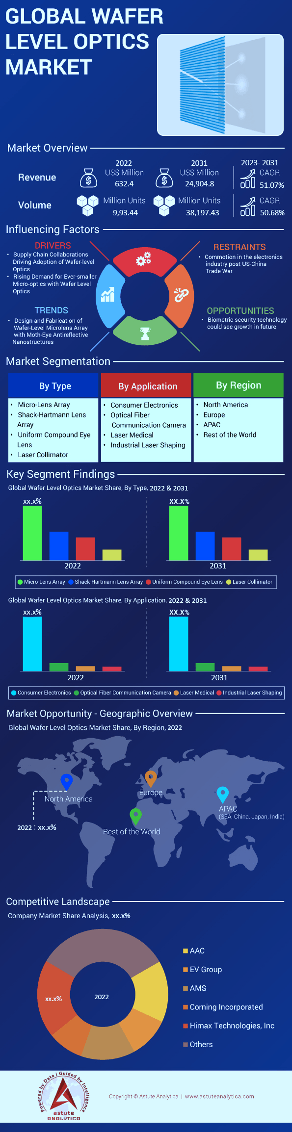
Global wafer level optics market is estimated to witness a major jump in revenue, from US$ 632.4 million in 2022 to US$ 24,904.8 million by 2031, at a CAGR of 51.07% over the projection period of 2023-2031. In terms of volume, the market is registering a CAGR of 50.68% during the same period.
The market outlook for wafer level optics is very promising as it continues to drive the advancement of the photonic technology industry. The ability to manufacture high-quality, precision optical components at a lower cost using semiconductor processes on wafers has opened up new opportunities for a wide range of applications.
Himax's wafer level optics technology is positioned to play a key role in shaping the future of sensing devices, AIoT, and machine vision. The technology's ability to manufacture micro-optic components for sensing applications, including refractive and diffractive optical elements and lightguides, has already revolutionized industries such as automotive, consumer electronics, healthcare, and industrial automation.
Furthermore, wafer level optics technology has enabled the development of advanced optical sensing solutions that are more accurate, compact, and cost-effective than traditional sensing methods. This has opened up new opportunities in fields such as autonomous vehicles, medical devices, and robotics.
To Get more Insights, Request A Free Sample
Market Dynamics
Growing Demand for Compact and High-Performance Electronic Devices
The demand for compact and high-performance electronic devices, such as smartphones, tablets, and wearables, has been growing rapidly in recent years. This trend is driving the demand for wafer level optics (WLO), which offer a compact and cost-effective solution for integrating optical components onto electronic devices. WLO allows for the miniaturization of optical components, which enables the development of smaller and more sophisticated electronic devices. This driver is expected to continue to fuel the growth of the WLO market in the coming years.
Increasing Demand for Optoelectronic Components in Various End-Use Industries
The demand for optoelectronic components, such as sensors, detectors, and light-emitting diodes (LEDs), is increasing in various end-use industries, including automotive, aerospace, healthcare, and consumer electronics. These components are used for a wide range of applications, such as imaging, sensing, and lighting. WLO technology allows for the integration of these components onto a single wafer, reducing the need for assembly and packaging, and resulting in cost savings and improved performance. The increasing demand for optoelectronic components is expected to drive the growth of the WLO market in the coming years.
Restraint
High Initial Capital Investment and Technical Expertise Requirements
One of the major restraints for the WLO market is the high initial capital investment required to set up a WLO manufacturing facility. The production of WLO requires specialized equipment and technical expertise, which can be expensive to acquire and maintain. Moreover, the process of manufacturing WLO involves several complex steps, including lithography, etching, and bonding, which require skilled personnel.
The high capital investment and technical expertise requirements can act as a barrier to entry for new players in the market and may limit the growth of the market to some extent. However, the increasing demand for WLO in various industries is expected to drive investments in the market, which could lead to the development of new technologies and reduced costs in the long run.
Segmental Analysis the Global Wafer Level Optics Market
By Type
Micro lens array is a type of wafer level optics that is used to manipulate light in various optical applications. These microstructures can be fabricated on a single wafer, allowing for cost-effective and high-volume production. The micro lens array segment is estimated to have the highest market share and is expected to exhibit the fastest CAGR of 52.27% during the forecast period.
The growing demand for high-quality imaging and display technologies, such as 3D imaging and displays, virtual reality, and augmented reality, is driving the demand for micro lens arrays in the consumer electronics segment. Additionally, micro lens arrays find applications in several areas of modern optics and optical products such as CCD arrays, optical microscopes, LiDAR systems, and optical sensors, among others, which in turn is escalating the segmental growth globally.
By Applications
The consumer electronics segment currently dominates the global wafer level optics market, while the laser medical segment is expected to witness the fastest CAGR of 52.3% during the forecast period. This is primarily due to the rising demand for laser surgery in various medical fields, such as ophthalmology, dermatology, gynecology, dentistry, urology, cardiovascular, and more.
The global wafer level optics market is experiencing high demand in the consumer electronics segment due to the growing adoption of advanced technologies, such as augmented reality (AR), virtual reality (VR), and 3D sensing, in smartphones, tablets, gaming consoles, and other electronic devices. Wafer level optics are used in these devices to improve their optical performance, reduce their size and weight, and enhance their functionality.
Wafer level optics can be integrated with other electronic components, such as sensors and processors, to create compact and high-performance systems. This makes them well-suited for consumer electronics applications that require advanced optics in small form factors, such as depth sensing, facial recognition, and gesture recognition.
Customize This Report + Validate with an Expert
Access only the sections you need—region-specific, company-level, or by use-case.
Includes a free consultation with a domain expert to help guide your decision.
To Understand More About this Research: Request A Free Sample
Regional Analysis
The Asia Pacific region has emerged as the largest market for wafer-level optics, with China leading the way in terms of revenue. The region's dominance in this market is attributed to the presence of several leading market players, including Himax Technologies, as well as numerous local players who are driving the growth of the industry.
The increasing adoption of wafer-level optics in various applications, such as consumer electronics, automotive, and medical devices, is expected to drive the market's growth in the region. The demand for high-quality imaging in smartphones, tablets, and laptops, is one of the major drivers of the market's growth in Asia Pacific.
Moreover, the growing initiatives by market players in India are expected to propel the region's growth rate over the forecast period. The Indian market is witnessing a surge in demand for wafer-level optics due to the increasing adoption of smartphones, tablets, and other consumer electronics products. In addition, the rising demand for advanced medical devices and the growing trend of automation in the automotive industry are expected to drive the market's growth in India. Several market players are focusing on developing innovative and cost-effective wafer-level optics solutions to cater to the increasing demand from these industries.
Furthermore, the Asia Pacific region is witnessing significant investments in research and development activities to enhance the performance and efficiency of wafer-level optics. The growing focus on technological advancements and product innovation is expected to further drive the market's growth in the region.
List of Key Companies Profiled:
- AAC Technologies
- China Wafer Level CSP Co.LTD
- Corning Inc.
- EV Group
- Himax Technologies, Inc.
- Largan Precision Co., Ltd.
- Tianshui Huatian Technology Co., Ltd.
- Zhuhai MultiscaleOptoelectronics Technology Co., Ltd.
- Other Prominent Players
Market Segmentation Overview
By Type:
- Micro-Lens Array
- Shack-Hartmann Lens Array
- Uniform Compound Eye Lens
- Laser Collimator
- Infrared Sensor
- Others
By Application:
- Automotive Front-Lights
- Light Carpets
- Optical Diffusers
- Medical Imaging
- Consumer Electronics
- Optical Fiber Communication Camera
- Industrial Laser Shaping
- Others
By Region:
- North America
- The U.S.
- Canada
- Mexico
- Europe
- Western Europe
- The UK
- Germany
- France
- Italy
- Spain
- Rest of Western Europe
- Eastern Europe
- Poland
- Russia
- Rest of Eastern Europe
- Western Europe
- APAC
- China
- India
- Japan
- Australia & New Zealand
- South Korea
- ASEAN
- Rest of Asia Pacific
- Middle East & Africa (MEA)
- Saudi Arabia
- South Africa
- UAE
- Rest of MEA
- South America
- Argentina
- Brazil
- Rest of South America
REPORT SCOPE
| Report Attribute | Details |
|---|---|
| Market Size Value in 2022 | US$ 632.4 Mn |
| Expected Revenue in 2031 | US$ 24,904.8 Mn |
| Historic Data | 2018-2021 |
| Base Year | 2022 |
| Forecast Period | 2023-2031 |
| Unit | Value (USD Mn) |
| CAGR | 51.07% |
| Segments covered | By Type, By Application, By Region |
| Key Companies | AAC Technologies, China Wafer Level CSP Co.LTD, Corning Inc., EV Group, Himax Technologies, Inc., Largan Precision Co., Ltd., Tianshui Huatian Technology Co., Ltd., Zhuhai MultiscaleOptoelectronics Technology Co., Ltd., Other Prominent Players |
| Customization Scope | Get your customized report as per your preference. Ask for customization |
FREQUENTLY ASKED QUESTIONS
The growth rate of the Global Wafer Level Optics Market is 51.07%, with an estimated value of US$ 24,904.8 Million by 2031.
The development of advanced optical materials requires extensive characterization of chemical, mechanical and optical properties as well as proven scalability for high-volume manufacturing (HVM).
Rising demand for ever-smaller micro-optics with wafer level optics and supply chain collaborations driving adoption of wafer-level optics is expected to boost the market for wafer level optics.
Commotion in the electronics industry post US-China Trade War inhibits the growth in the Global Wafer Level Optics Market.
Micro-Lens Array segment contributed the major share in the global wafer level optics market in 2022.
The recent trends in the semiconductor industry such as thin-wafer handling, 3D-IC/TSV, subwavelength metal gratings for color filtering in CMOS technology and others will have a significant impact on the prospering micro-optics industry in the near future.
China holds a major share in term of revenue in the global wafer level optics market in 2022.
Types and application are the different segments of the global wafer level optics market.
Consumer Electronics segment is expected to project the highest CAGR of 52.3% in the global wafer level optics market during forecast period.
Some of the key players operating in the global wafer level market include AMS AG, Himax Technologies, Inc., EV Group, Corning, China Wafer Level CSP Co., Ltd. and AAC Technologies among others.
LOOKING FOR COMPREHENSIVE MARKET KNOWLEDGE? ENGAGE OUR EXPERT SPECIALISTS.
SPEAK TO AN ANALYST
.svg)


Features | Type of License | ||||
Data Book | Single User |   Multi User | Corporate | ||
| e-Access | ✓ | ✓ | ✓ | ✓ | |
User Sharing | 1 User Only | 1 User Only | Up to 7 Users | Unlimited User Access | |
⨉ | ⨉ | ⨉ | ✓ | ||
Free Customization | No Free Customization | Up To 30 hrs work | Up To 60 hrs work | Up To 80 hrs work | |
Deliverable |
| ⨉ | ✓ | ✓ | ✓ |
| ✓ | ⨉ | ✓ | ✓ | |
| ⨉ | ⨉ | ⨉ | ✓ | |
Analyst Support | 2-Months Analyst Support | 4-Months Analyst Support | 7-Months Analyst Support | One Year Analyst Support | |
Free Report update in next update cycle | ⨉ | ⨉ | ⨉ | ✓ | |
Free Industry Update (Within 180 days) | ⨉ | ⨉ | ⨉ | ✓ | |
Benefit | Up to 10% off on Post Purchase | Up to 20% off on Post Purchase | Up to 30% off on Post Purchase | Up to 40% off on Post Purchase | |